Intro
I have been done some work on valve amps. And I did search the market for voltage regulators with high ripple rejection rate. And currently at market there is high voltage regulator LR8, with ripple rejection rate at -60db. But for quality audio, this is too noisy. The other solutions would be to use HIP5600 regulator (which is sadly discontinued now), this offered -72 db output voltage ripple regulation.
The voltage regulator
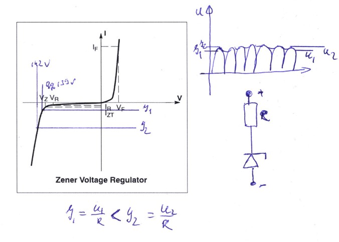
But my idea was to build my own voltage regulator with high ripple rejection rate. I was looking on zener diodes which for some reason are referred as “noisy”. But I was thinking why they tend to be noisy. And my conclusions was that when the unregulated voltage peaks, the current source resistor increases the current over the Zener (by Ohm law I=U/R). Increased (or fluctuating) current makes the zener diode generate some differences in the output voltage.
The classical zener connection:
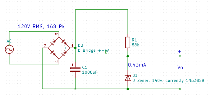
Here Vout will fluctuate as the peaks of the on the input causes current changes in (R1) and current changes generates slight voltage changes over the Zener diode. As the chart of the diode is not perfectly vertical at conducting point in respect to current. Thus here is the concept diagram of the processes which actually are happening with Zener during consumption of unregulated voltage:
To avoid the current changes, I have an idea to use a const current source instead of R1 load. This will fix the zener diode in singe voltage point. With this we can reach nearly “perfect” ripple rejection. Zener voltage might float due to temperature changes, but for valve amplifier this is not a problem. Most significant is to avoid the ripple at any price. Thus idea is to use CCS (single DN2540 for example seems to be good for this purpose, but cascade might give even better results…) as the load for the Zener diode.
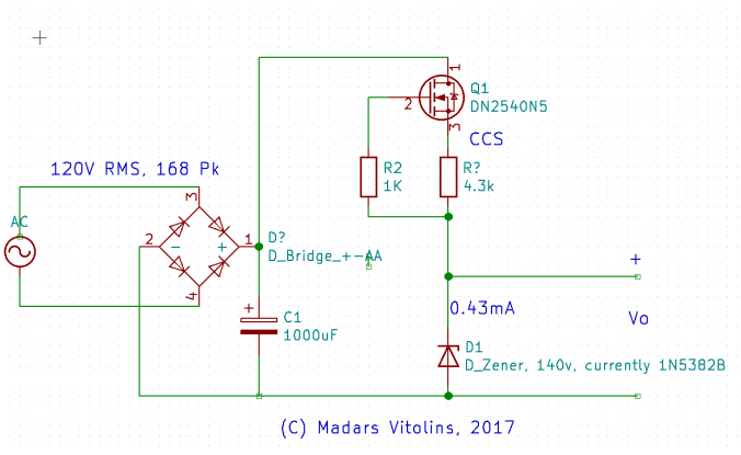
In Multi-Sim the regulation the zener diode noise is around -84 db (with Mosfet load, see next scheme). While with restive load the noise is -58 db. Which is significant difference. This gives advantage of the -26 db! Which is a quite a lot (more that 10x) lower ripple voltage.
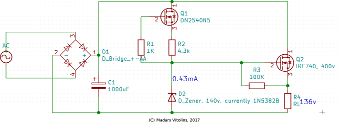
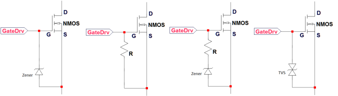
When reference voltage have been established, we need to make some power output. For example 130v, 300mA. To do this, we could use BJT in common emitter mode (or Darlington in the same mode, Darlington is recommended because of lower base current requirements). But problem with BJTs are that current is needed. For example for driving MOSFETs, current is not needed. Thus we could use N channel Enhancement MOSFET in common source configuration. Only problem here is with the Gate-Source voltage. Typically it is about +/- 20v. But at startup we provide to gate 130v, and at that point at mosfet source there could be still 0 volts, thus delta will be greater than 20v, which will damage the transistor (i have burn’t 3x of IRF740…). Thus to avoid this, we could use some resistor between gate and source with high resistance. For example 100K ohm. This will ensure that at startup source and gate is at the same levels. But when the load will start to conduct, the the voltage across the resistor will fall, thus gate will be at higher potential than source, and the MOSFET will start to open. And in the same way opposite, if we receive some peak value from the unregulated output, the MOSFET source will become more positive than gate, and MOSFET will slightly close. IRF740 MOSFET is fine for this purpose. Thus the final scheme looks like:
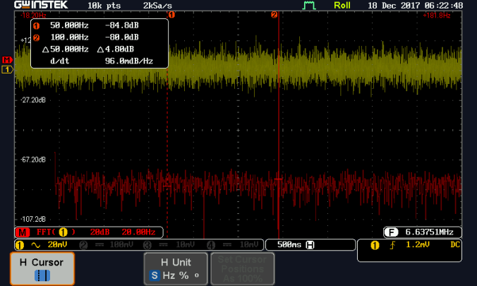
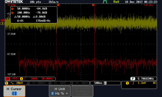
The output spectrum with ~200mA load looks looks like (log). The 100Hz regulation occurs from -75db to -85db and the same for 50Hz. But here question is too about how good are scope readings. As they look the same for other frequencies too… Also I have found that if Zener diode becomes hotter, at some point there is excessive noise even with CCS in series. For this reason 0.43mA is fine, the Zener stays cool. Thus If you need some high voltages or higher current on Zener diode, then maybe it is good idea to connect Zeners in series so that there are bigger surface for heat dissipation.
AC mode readings from the load
Update 23/12/2017
It looks like for output MOSFET other techniques can be used to protect gate source overvoltage at start moments. See https://electronics.stackexchange.com/questions/187075/mosfet-gate-source-protection-question

What about +275v output, 150ma? Just change zeners to series? Thanks, James
LikeLike
Yep should work with some series of zeners for D1. Regarding the currents, just check how much you plan to feed from the mains, if some 300v, then it will be then Q2 will dissipate 300-275=25*0.15A = 3.7W. Some heat-sink will be needed.
LikeLike